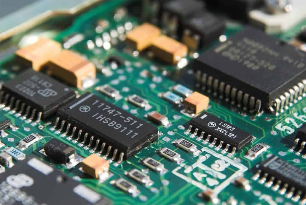
Tips For Creating Secure PCB – For a PCB manufacturer, the security factor of the board gives them a lot of headaches. Everyone tries hard to make their work secure, but the reality is it’s not that easy work to get rid of cybercrime.
A hundred percent security is next to impossible in this world full of cyber hackers.
But with some precaution measures, you can control it to the minimum level. As device security is very vulnerable, IoT has to protect their conversations and have to be encrypted. To be secure from the black hacker or reverse-engineering, some higher level of protection ought to be mandatory.
In both fields, hardware and software, protection is required. These protection measures are needed from the beginning of manufacturing. A special team is needed to look after the safety measure. From first to the end of the manufacturing, these teams are concerned about the device’s security keenly.
Keep Your Data Safe
If you can hide the sensitive database from the hacker, you can protect your device from crime. When hackers somehow access your board, they reverse engineer your board design and snatch all data. Here, in this article, we inform how you can protect your device and keep your data safe.
Don’t share your database with anyone unknown. When you need to share information, make them encrypted. Whenever you share your data with your co-workers, make sure that it is confidential.
Some processes like using unique chips, using silicon remedy for designing, scratching off the chips, etc., are some techniques to protect the device. Not only in software but hardware also you have to take steps. Below are some security procedure to create a secure PCB procedure:
- Reduce The Test Points
Test points are the area of the junction of the interconnection. Test point evaluates the integrity of the PCB assembly board through an automatic test sequence. If you cut down the unnecessary test point, it will be harder for the hacker to duplicate the design.
There are two test points: an in-circuit test point, and the other is a flying probe test point. If reduced in both types of test points, your machine will become more secure.
Although all points are too probable to cut out, you can use a copper pad at the junction to conceal the connection. This copper pad prevents outsiders from stealing information from point-to-point.
- Protect Crucial Traces In The Internal PCB Layer
You can hide the most critical traces in between two layers of the copper plate. It will not be noticeable, so hard to track. As it is invisible from the outside, reverse engineering becomes harder. It decreases the potential probing threshold for the hacker.
- Use Buried Vias Or Blind Vias For Routing
You can avoid the chance of hacking in the routing process also. You can do routing by two processes, either by buried vias or by blind vias. In the case of buried vias, the top and the lowermost layer avoid tracing. And in blind vias, traces are buried in between the inner layers, so they cannot be seen from the outside layer. By these two methods, the attack is lessened to some extent.
- Minimize The Electrical Noise
Noisey signal lines should be separated away from sensitive traces. Hackers have advanced technology that can easily detect noisy signals. So be cautious from noise electrical signals. If you can use the proper power supply and grounding, EMI emission reduces some level which lessens the noise.
- Use Advance Packaging
Your advanced packaging is also an option to protect from cybercrime. Limit your packaging to secure X-ray vision. If the device’s packaging is such that a hidden connection is located in its hidden layer, it will be challenging for the attacker to access data.
When X-ray vision is applied, it is hard to detect, probe, manipulate. This X-ray vision might be a little expensive, but it will protect your board integrity. Some examples of advanced packaging services are Chip-on-board, Ball Grid Array, etc.
- Align The Separation Line In Parallel
A parallel line is easy to hide traces. They conceal the visibility of the probe by sandwiching them in between the middle layer. Besides that, it reduces the noise of the electronic power supply and enhances the dynamic expanse.
- Use Plastic Casing To Secure The PCB Board
A rigid case can protect your PCB board, especially if it has a sensor. External shells act as the safeguard of the device. Hide the internal circuit board so its mechanism can’t be seen from outside. A signal inhibiting glue or adhesive is used to fix the board. Not only these, but it also prohibits all signals to come. So the attacker can’t hack it.
- Turnkey PCB Assembly
If you don’t have time to look after so much stuff to secure your device, you can hire a turnkey PCB assembly. From A to Z, it will provide all services to your device. It supplies the service of security also. They have a special team for each sector, so as for hacker management also. So you can relax by giving them the responsibility of your device.
Their team is experts in handling such cases of reverse engineering. They know very well how to obsolete hacking completely from your device.
And the best part is with the security they also give every service from designing, constructing, and delivery.
So, use the benefits of a ready-made remedy to protect your machine from the dark world using turnkey PCB assembly.
Creating Secure PCB – Conclusion
As crime increases day by day, the protection steps have to be more powerful than usual. Try to understand where missing in the protection lies; try to chop it down. Comprehend the technology of that wide world of hacking because they are very smart. They evolve with advanced technology. So it’s time to update your manufacturing process too.
Above are some ways to secure your device from reverse engineering. There are many techniques to reap hacking. We discussed some very important routes among them. Try to apply them to your device if you don’t want to face a hacker in the future.