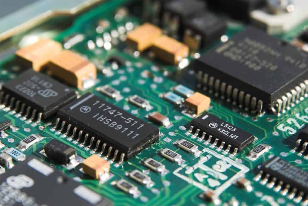
A Multilayer PCB has at least three or more conductive layers, and the electrical connection between these conductive layers is achieved using through-hole vias blind or buried vias. With the technological growth in the electronics domain, the demand for complex PCBs has increased enormously. Multilayer PCBs offer several advantages like compact size, improved robustness, high assembly density, lightweight, etc. These advantages make them the best choice in almost all the electronic applications ranging from customer electronics, telecom, automotive, medical equipment, satellite communication, and many more.
Multilayer PCBs usually include at least three conductive layers of double-sided circuit boards. They are laminated and glued with heat-protective insulation layers between them.
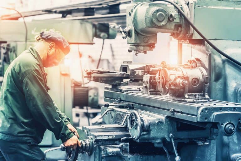
We shall briefly discuss the manufacturing process of a Multilayer PCB before discussing the significant challenges faced by the PCB experts. Once the circuit design is completed and ready for PCB fabrication, the below steps are followed:
- Print the circuit design
A negative image is developed and printed on transparent film. Registration holes are pressed to keep the layers aligned.
- Print the copper for the interior layer
To print the inner layers, copper is re-bonded to the laminate piece to serve as the PCB structure.
- Remove unwanted copper
An effective chemical is used to remove the extra copper that is not covered by the photoresist, leaving only the required copper on the PCB.
- Laminate the PCB layers
The fault-free layers are fused by first laying up and then by laminating.
- PCB drilling
The PCB drilling is done based on the pre-set drill spot using an X-ray machine to keep the stack intact.
- PCB plating
In this process, different PCB layers are fused using a chemical, and further, a layer of copper deposition is done.
- Outer layer Imaging and plating
A photoresist is applied to protect the copper deposited on the outer layers, followed by a tin plating.
- Final etching
The tin plating protects the required copper during this stage. The unwanted and exposed copper is etched out, and the PCB connections are properly established.
- Solder mask
The cleaned PCB panels are exposed to UV light with an applied epoxy solder mask ink. Further, the board passes through an oven to cure the solder mask.
- Surface finish and silk-screen
PCB plating is done with gold or silver to increase the solderability of the components on the PCB. Ink-jet silkscreen writing is done in this stage, followed by the final coating and curing process.
- Electrical test
Technicians perform electrical testing to confirm the functionality of the PCB.
- Profiling and cutting
In this last step, PCBs are cut out from the panels, and a board inspection is done before packing the PCBs for shipment.
Knowing the various steps of manufacturing a multilayer PCB, we shall now consider the major difficulties faced during the process.
- Mechanical distortions like Bows and twists are common during multilayer PCB fabrication. These errors affect the board flatness, which further creates assembly issues like component mounting, solder paste deposition, etc. Using correct parameters while pressing the multilayer PCB can reduce the board distortions, and choosing similar substrate materials can provide uniform fusing of layers during fabrication. Manufacturers should use appropriate machinery and follow the necessary guidelines while pressing multilayer PCBs.
- Thermal and Electrical problems due to incorrect selection of substrate material is another majorly faced challenge in it. These PCB materials conduct electricity and also provide insulation between the copper layers. Choosing versatile substrate materials like FR4 can provide the best electrical insulation.
- Delamination can happen more frequently in multilayer PCBs as the potential areas rise with the increase in layers. Copper laminates detach on surfaces or in internal layers if the copper foil doesn’t have high peel strength. This failure is quite tricky to fix and may need a re-spin.
- Moisture penetration in the board can cause damage and disrupt the functionality of a Multilayer PCB. The substrate chosen should have a low hygroscopic value. Any contamination in the circuit board may cause component or signal shorts that may degrade the PCB performance.
- Drilling precision is critical in Multilayer PCBs as the bottom layer of the stack up will have larger holes than the internal layers. Back-drilling is used in multilayer PCBs to reduce the number of parasitic elements generated by plated through holes. But the associated challenges with this drilling technique are stuck pipe, hole cleaning, and loss of circulation.
- Via type chosen in multilayer PCBs can cause challenges to the contract manufacturer. The high precision required in drilling blind or buried vias can be difficult in Multilayer PCBs.
- Due to the dense component design, mounting heat dissipation components can be a challenge in Multilayer PCBs. Choosing effective components with planned thermal design is a must in multilayer PCB manufacturing.
Multilayer PCBs offer many advantages like small size, high speed, and reliability. Hence manufacturers are finding new techniques to overcome the difficulties faced during the PCB manufacturing process. But there are certain disadvantages also in using Multilayer PCBs like higher cost, complex production techniques, need for skilled design and assembly staff, etc.
With all these advantages and disadvantages, Multilayer PCBs are still the most sought-after PCBs in applications like
- Medical devices like CAT scans, X-ray machines, and other diagnostic equipment
- Consumer electronics like smartphones and high-tech gadgets
- Satellite and defence equipment
- High-speed telecom devices
- Latest IoT applications
With the technological innovations, the volume of multilayer PCBs is going to expand. Many contract manufacturers have invested in these growing trends and are focusing on providing high-quality fabrication services for Multilayer PCBs. CMs are tackling the major difficulties faced during the manufacturing process of Multilayer PCBs effectively by using the latest fabrication process and production machinery. You can build a high-performance multilayer PCB by collaborating with a CM who has experience in handling such challenges and has demonstrated success in producing Multilayer PCBs.